FOR IMMEDIATE RELEASE
Hitachi High-Tech Launches DCR Etch System 9060 Series, Supporting Isotropic Etching of Advanced 3D Devices at the Atomic Level

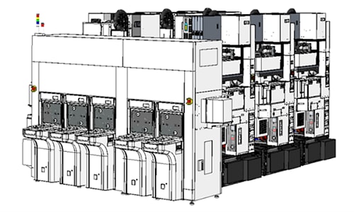
DCR Etch System 9060 Series
Tokyo, November 27, 2024 – Hitachi High-Tech Corporation ("Hitachi High-Tech") announced today the launch of its DCR*1 Etch System 9060 Series. This system, which leverages Hitachi High-Tech's plasma etching*2 technology and expertise, has been developed to achieve precise control over the horizontal (isotropic) etching process in dry environments, aimed at applications such as the high-aspect*3 three-dimensional structures used in advanced semiconductor devices.
With the 9060 Series, Hitachi High-Tech will support manufacturing process advancements for cutting-edge semiconductor devices, which are becoming increasingly minute and more complex, and will help customers to overcome the challenges they face, from R&D through to mass production.
*1 DCR (dry chemical removal): A method used to advance both vertical and horizontal etching by utilizing chemical reactions in a dry environment.
*2 Plasma etching: A technique used to fabricate detailed patterns using ions and chemical reactions by separating gases in a vacuum chamber.
*3 High-aspect: Generally, refers to the aspect ratio of a rectangle. Here, it refers to the ratio of depth to width (depth/width) of patterns to be etched on wafers. A high aspect means this ratio is a high value, which makes it very difficult to manufacture and measure.
Product Development Background
Semiconductor devices have become increasingly miniaturized over the past half century and beyond, with the processing dimensions of integrated circuits now at nanometric levels. This, in turn, necessitates controllability over the etching process at the atomic-layer (angstrom) level. In addition, the likes of 3D-NAND*4 and 3D-DRAM*5 structures are used for semiconductor memory devices to improve density by making the elemental structure three-dimensional. As a result, the dry etching process used to manufacture semiconductor memory devices requires isotropic (horizontal, even) etching, which is precisely controlled at the atomic-layer level, in addition to conventional anisotropic (vertical) etching.
The 9060 Series maintains the low-damage, high-precision plasma etching technology cultivated by Hitachi High-Tech over many years while achieving isotropic etching at the atomic-layer level, thereby helping our customers who manufacture advanced semiconductors with highly integrated three-dimensional structures by shortening development periods, reducing costs, and improving productivity.
*4 3D-NAND structure: A type of non-volatile flash memory. Refers to a NAND flash memory in which memory cells are arranged vertically as well as horizontally to increase storage density.
*5 3D-DRAM structure: A type of volatile memory. A structure in which bits are stored vertically to achieve high density.
Key Features
1. Achieves high throughput processing and low equipment footprint*6
Typically, when performing isotropic etching in dry environments, it is necessary to alternate between low temperatures for adsorption of radicals*7 and high temperatures for thermal desorption, which means time is required for heating and cooling. To resolve this problem, the 9060 Series incorporates a unique wafer-cooling mechanism and infrared lamp within a single vacuum reactor, enabling the temperature of the wafer being etched to quickly alternate between low and high temperatures. This enables high-throughput isotropic etching of various materials and lowers the footprint of the equipment.
*6 Footprint: The amount of space taken up by a piece of equipment.
*7 Radical: An atom or molecule with unpaired electrons. Characterized by high reactivity.
2. Achieves high-precision isotropic processing
In addition to isotropic processing through heating and cooling via the wafer-cooling mechanism and infrared lamp, the system also utilizes plasma etching technology—one of Hitachi High-Tech's strengths—to achieve isotropic processing with high surface reaction speed and highly precise control. This makes it possible to control the shape of the openings and bottom of the wafer pattern at the atomic level, which is essential to fabricate detailed three-dimensional structures.
With the 9060 Series as well as our other high-performance etch systems and technology, Hitachi High-Tech is continuing to respond to our customers' various manufacturing needs for the development and mass production of semiconductor devices.
We will continue to provide innovative and digitally enhanced solutions to our products for the upcoming technology challenges, and create new value together with our customers, as well as contributing to cutting-edge manufacturing.
About Hitachi High-Tech
Hitachi High-Tech, headquartered in Tokyo, Japan, is engaged in activities in a broad range of fields, including manufacture and sales of clinical analyzers, biotechnology products, radiation therapy systems, semiconductor manufacturing equipment, analytical instruments, and analysis equipment. Also, we provide high value-added solutions in industrial fields such as mobility, connected, environment and energy, etc. Through business based on our core Observation, Measurement and Analysis technologies, we will contribute to the realization of a sustainable society by solving social issues.
The company's consolidated revenues for FY2023 were approx. JPY 670.4 billion. For further information, visit https://www.hitachi-hightech.com/global/en/
Contact
Kazuki Higashiyama
Process Marketing & Planning Dept.,
Semiconductor Manufacturing Systems Div.,
Nano-Technology Solution Business Group,
Hitachi High-Tech Corporation
E-mail: kazuki.higashiyama.wt@hitachi-hightech.com
