Shinya Kudo
Scanning probe microscopes (SPMs/AFMs) are instruments in which an extremely sharp probe tip, mounted on the end of a cantilever, is scanned over the surface of a specimen while the cantilever displacement—a measure of the strength of interaction between the probe tip and the specimen surface—is recorded, yielding images reflecting the morphologies and physical properties of specimen surfaces.
SPMs and AFMs can operate in a wide range of environments—in vacuum, under ambient conditions, in liquids, and more—and can offer not only high-magnification observation and measurement of three-dimensional surface morphologies, but also information on the physical properties of specimen surfaces. For these reasons, scanningprobe instruments have become essential tools for nanometer-scale R&D and quality control of specimens in a wide range of fields, including organic and macromolecule substances such as plastics, rubbers, and blended polymers, semiconductors, inorganic materials, magnetic memories, and living organisms. In recent years, progress in nanofunctional materials and thin films has created growing demand for analytical instruments with greater sensitivity and higher resolution.
The AFM100 series of multifunctional scanning probe microscopes features a three-instrument lineup (Figure 1). The basic model is the tabletop AFM100, while the mid-range AFM100 Plus and high-end AFM100 Pro add additional system components to support a broader range of measurement objectives and spatial resolutions.
In this article we survey key features of the AFM100 series, then present sample applications to illustrate its capabilities.
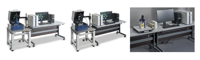
Fig. 1 The AFM100 series of multifunctional scanning probe microscopes. Left: AFM100 Pro, Center: AFM100 Plus, Right: AFM100.
The acquisition of AFM images proceeds on a line-by-line basis: after measuring one full line, the tip is moved to the next line and the process repeats. Consequently, acquiring images—particularly high-resolution images—requires long measurement times, over the course of which thermal drift can give rise to distortions in measured images, degrading data reliability.
To address this difficulty, instruments in the AFM100 series are equipped with thermal suppression units that eliminate all stray heat sources, reducing thermal drift to below 0.03 nm/s—a reduction of more than 70% compared to previous-generation instrument models.
This mitigates issues such as blurred or distorted images caused by thermal drift resulting from continuous (time-lapse) measurement of a single sample region.
Figure 2 compares images acquired by the AFM100 Plus and by a previous-generation instrument for a 120-min time-lapse measurements of a particulate specimen. Whereas the image acquired by the previous-generation instrument shifts significantly over the course of the measurement period, almost no shift is visible in the AFM100 Plus images.
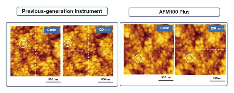
Fig. 2 Time-lapse measurements of particulate sample.
The scan parameters for AFM systems must be re-calibrated whenever the cantilever or the measurement specimen is changed. One consequence is that the trustworthiness of measured data may vary significantly depending on the extent of the operator's experience and technical skill. Also, before making measurements it is necessary to replace the extremely small cantilever, a painstaking procedure that imposes a heavy burden on users preparing to make measurements.
To address these difficulties, AFM100-series instruments are equipped with a premount holder that enables a simple one-touch procedure for replacing cantilevers (Figure 3), as well as an autopilot function (Figure 4) allowing measurements to be made via preconfigured recipes. These features not only reduce the dependence of measurement quality on operator expertise, but also increase total measurement throughput.
In addition, combining the autopilot function with RealTune II—a system for automating the setting of scan parameters—enables measurements to be made at multiple measurement points with optimal scan parameters for each point configured automatically. This allows the acquisition of highly reliable data—independent of operator skill and experience—with just a single mouse click.
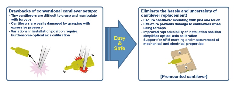
Fig. 3 Conceptual diagram illustrating premount specimen holder.
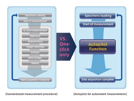
Fig. 4 The autopilot function automates many of the steps required by previous-generation instruments.
After performing wide-area measurements of a specimen, the autopilot function allows users to specify multiple specimen locations for automated measurement and analysis. Figure 5 shows an example in which the autopilot was invoked to automate measurements at multiple points on a specimen of silica particles adhering to a Si substrate, after which the measured data was subjected to an automated roughness analysis.
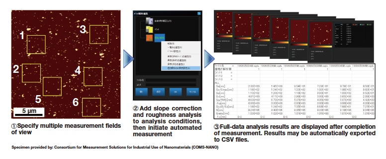
Fig. 5 Automated measurements at multiple points on silica-particle specimen.
To support SÆMic (scanning electron microscopy (SEM)/AFM correlated microscopy) analysis—which was previously available only to users of the AFM5500M intermediate-scale probe microscope system equipped with a motor-driven stage—the AFM100 series offers AFM marking to allow SEM and AFM observation of identical sample regions on smaller instruments.
AFM marking uses a specialized cantilever to create marks on specimens indicating AFM-observed regions. These marks can then be used as guides in SEM measurements, allowing the same regions to be observed with ease. Parameters governing the creation of marks may be configured via control software, facilitating the process of marking specimens by proceeding in accordance with an operational flow. Also, because this process requires no specialized specimen stage, any SEM system may be used for SEM observation of previously AFM-observed regions.
Figure 6 shows an example in which AFM marking was used to acquire AFM and SEM images of a single region of a polished duralumin (A2017) surface. In general, compared to other aluminum alloys, duralumin exhibits superior strength but inferior corrosion resistance. Characterizing the corrosion resistance of a specimen requires identifying nonuniformities in the electric-potential distribution across a metal surface and determining the factors responsible for creating these nonuniformities. To this end, we used Kelvin probe Force Microscopy (KFM) to acquire simultaneous morphology images and electric potential images of a surface region via AFM, and then acquired energy dispersive X-ray spectroscopy (EDX) mapping images of the same surface region via SEM. Comparing these images suggests that high-contrast regions in electric-potential maps result from inclusions containing Si, Cu, Fe, or Mn, thus providing insight into the factors affecting corrosion resistance.
Adding AFM-marking capabilities to small-scale AFM systems extends to such systems the ability to capture simultaneous SEM and AFM images of identical sample regions, enabling easy analysis and characterization of surface morphology, material composition, and element distributions via SEM together with information on 3D morphology, mechanical properties, and electromagnetic properties via AFM, in the same field of view.
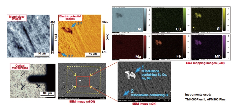
Fig. 6 Images of single region of aluminum alloy observed by AFM100 Plus and by TM4000 Plus II.
The AFM100 Pro extends the base functionality of the AFM100 by increasing the sensitivity of the cantilever displacement detector and adding a newly designed optical head that uses photothermal excitation to vibrate the cantilever. This result is a premium-grade instrument optimized for improved sensitivity in measurements of physical properties and at atomic and molecular scales.
The high-sensitivity optical head of the AFM100 Pro features a completely redesigned cantilever-displacement detector. With a high-frequency modulator to reduce mode-hopping noise in the high-power laser and reduced shot noise in the optical detector, the new detector reduces the noise level for displacement detection below 35 fm/√Hz—thus increasing sensitivity by approximately 8-fold compared to the previous-generation optical head. This greater sensitivity provides a higher signal-to-noise ratio for measurements of physical properties requiring detection of ultra-weak forces and ultra-small displacements.
As one illustration of increased sensitivity in physical-property measurements, Figure 7 compares AFM100 Plus and AFM100 Pro measurements of the distribution of polarization domains in a (Na,K)NbO3 specimen. These measurements were made using Piezo-Response Microscopy (PRM), in which an AC voltage applied between the probe tip and the specimen induces piezoelectric strain in the specimen, which is characterized and plotted by measuring the cantilever displacement.
The AFM100 Pro signal is less noisy than that for the AFM100 Plus, allowing high-sensitivity observations of polarization states even for minuscule domains.
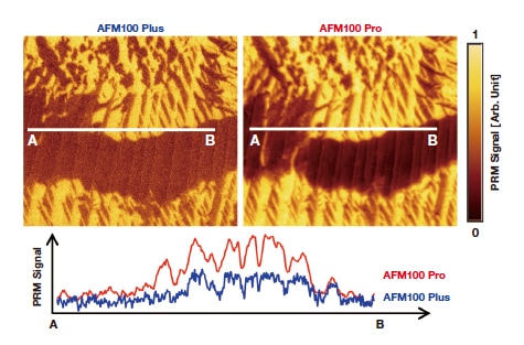
Fig. 7 Comparison of AFM100 Pro and AFM100 Plus measurements of distribution of polarization domains in (Na,K)NbO3 specimen.
Sample provided by: Professor Kenichi Kakimoto, Graduate School of Engineering, Nagoya Institute of Technology
The cantilever system of the AFM100 Pro adopts a new approach to cantilever excitation: the method of photothermal excitation (IR drive), in which laser light impinging on the back side of the cantilever is power-modulated to create thermal deformations that induce vibrations in the cantilever.
In contrast to the conventional piezo-drive approach—in which the cantilever is mechanically vibrated by a piezoelectric element—the IR-drive approach allows direct excitation of the cantilever itself, eliminating susceptibility to vibrations in neighboring components and allowing stable vibration with an ultra-small amplitude of sub-nanometer order.
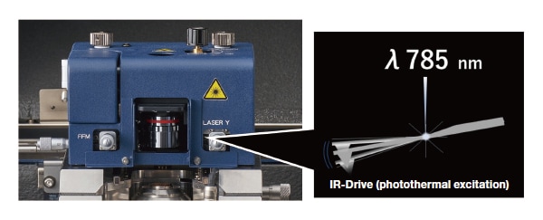
Fig. 8 Photothermal excitation.
The conventional approach to cantilever excitation was especially troublesome for operation in liquids, where the viscous resistance of the liquid and other factors complicated attempts to achieve stable vibration. In contrast, the IRdrive approach enables ideal states of cantilever oscillation that remain stable over long periods of time, even in liquids.
Figure 9 compares the resonance properties (Q-factor) of a typical cantilever excited via IR-drive and piezodrive approaches in a liquid environment. Whereas the piezo-drive approach produces multiple auxiliary peaks and considerable signal noise, the IR-drive approach yields a nearly ideal resonance curve with low noise and a single resonance peak, even in a liquid environment.
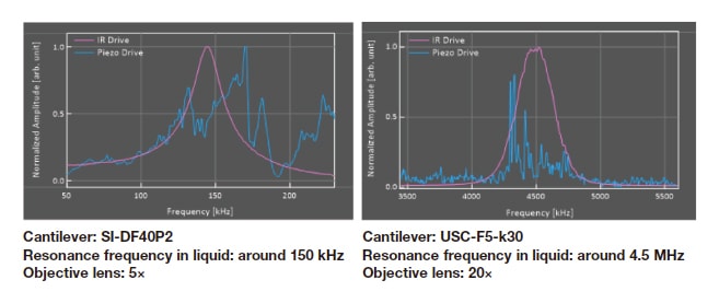
Fig. 9 Cantilever resonance curves measured in liquid.
As one example of a high-resolution measurement made possible by the use of photothermal excitation to achieve stable cantilever vibration with sub-nanometer-order amplitude, Figure 10 shows the results of an atomic-scale DFM measurement of a single-crystal calcite specimen in liquid. The measured image successfully captures ordered arrays of atoms in the crystalline structure of the specimen; the lattice dimensions extracted from the measured data are 0.86 nm × 0.58 nm. The atoms observed in this image lie on the outermost surface of a cleaved (104) plane of the calcite specimen; the crystal orientation is indicated by rectangles in the figure.
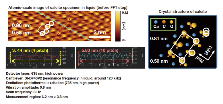
Fig. 10 Atomic-scale measurement of crystalline structure in calcite specimen in liquid.
In this article we surveyed key features of the AFM100 series of multifunctional probe microscopes and the high-end AFM100 Pro model, and then presented sample applications illustrating the capabilities of these instruments.
All instruments in the AFM100 series boast improved drift behavior and other basic performance enhancements, a premount holder to simplify cantilever installation, and autopilot functionality to reduce or eliminate measurement errors caused by instrument operators. These features will improve data reliability and increase operating efficiency, especially for quality-control applications. The addition of AFM marking support allows close interoperation with SEM systems while retaining the advantages of probe microscopy (3D morphology analysis and measurement of physical properties), opening a world of possibilities for developing new material-analysis solutions based on probe microscopes.
In addition, the AFM100 Pro features a completely redesigned displacement detector—offering improved sensitivity and lower noise—and a new photothermal mechanism for cantilever excitation enabling stable vibration with ultralow amplitudes of sub-nanometer order. This will allow AFM systems to be used for characterization of structural and physical properties in new classes of specimens—including advanced materials with ultra-miniature features (nanofunctional materials), thin films, and organic matter.
Acknowledgements
The high-sensitivity optical head for the AFM100 Pro was developed with guidance from Professor Takeshi Fukuma of Kanazawa University.
About the authors
Shinya Kudo
Focused Ion Beam Systems Design Dept.
Beam Technology & Analytical Systems Product Division
Core Technology & Solutions Business Group
Hitachi High-Tech Corporation