| Company Name | Japan Fine Ceramics Co., LTD. |
|---|---|
| Location | Sendai, Miyagi, JAPAN |
| Established | April 5, 1984 |
| Capital | 300 Million Yen |
| Net Sales (FY ended 3/30/2019) |
8,800 Million Yen |
| Number of Employees | 460 |

| Material | Alumina 99.90% |
Alumina 99.50% |
Alumina 96% |
AlN | Alumina (Black) |
|
|---|---|---|---|---|---|---|
| Bulk Density [g/cm3] | 3.9 | 3.9 | 3.8 | 3.3 | 3.7 | |
| Flexural Strength [MPa] | 660 | 440 | 300 | 330 | 320 | |
| Coefficient Liner Thermal Expansion [1/K] | 25 ~ 800℃ | 8×10⁻⁶ | 8×10⁻⁶ | 8×10⁻⁶ | 4.6×10⁻⁶ | 8.3×10⁻⁶ |
| Thermal Conductivity [W/m・K] | 25℃ | 33 | 32 | 23 | 170/200/230 | 21 |
| Young's Modulus [GPa] | 390 | 380 | 340 | 330 | - | |
| Poisson's Ratio [-] | 0.25 | 0.25 | 0.23 | 0.24 | - | |
| Dielectric Constant (25℃) [-] | 1MHz | - | - | - | 8.8 | 8.5 |
| 10GHz | 10 | 9.8 | 9.6 | - | - | |
| Dielectric Loss angle (25℃) [-] | 1MHz | - | - | 2×10⁻⁴ | 5.0×10⁻⁴ | 3.5×10⁻⁴ |
| 10GHz | 1×10⁻⁴ | 1×10⁻⁴ | - | - | - | |
| Volume Resistivity [Ω・cm] | 1015 | 1015 | 1014 | 1012 | 1014 | |
| Surface Roughness (Ra) [μm] | 0.02 | 0.02 | 0.3 | 0.05 | 0.3 | |
| Thickness [mm] | 0.05 ~ 0.38 | 0.15 ~ | 0.5 | 0.1 ~ | 0.15 ~ | |
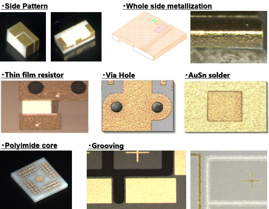
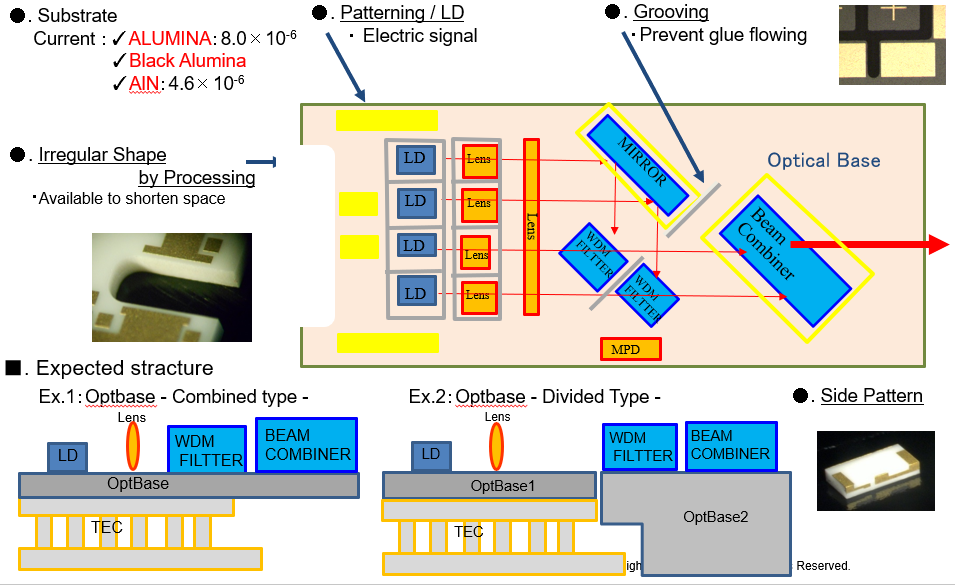
We make submount according to your design.

The material near the heat expansion coefficient of an optical component can be chosen.


Characteristics of discrete semiconductor devices are often undermined due to the heat that is generated from inside module. To solve this, mounted substrates require heat dissipation, electric insulation and CTE which matches semiconductor chips.