
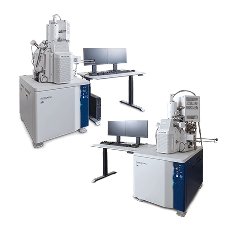
High Resolution Schottky Scanning Electron Microscope
SU3900SE/SE Plus SU3800SE/SE Plus
SE Series Offering a Combination of High Performance and Versatility
The SU3900SE/SU3800SE Series Microscopes are FE-SEMs that offer high-resolution observation capabilities. They combine easy data acquisition through simple operation with much larger and heavier specimens than existing FE-SEMs. This makes it possible to observe large and heavy specimens including industrial materials such as iron and steel, automotive parts, and aerospace-related parts.
Furthermore, the SE Series lineup offers four models (two types with two grades) to meet the measurement needs of a wide variety of fields.
Each model provides unique capabilities; for example, the large-chamber models provide the best results for foreign matter and defect analysis, helping drive quality and yield. While the Plus models are ideal for the observation of fine surface structures, creating opportunities for improvements in electronic components and semiconductor manufacturing.
* The device photograph shows configuration with optional items.
Features
●Schottky SEM with large specimen chamber to expand application capabilities
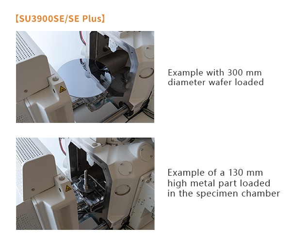
Evaluating shapes by electron microscopy is the foundation of all material evaluation and analysis. Demand has always existed for the ability to mount and observe specimens in their original shape.
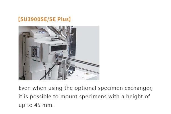
The SU3900SE/SU3800SE Series Microscopes have a highly rigid multipurpose specimen chamber that makes it possible to mount specimens as is.
This eliminates the need to perform metal coating of non-conductive specimens and breaking or cutting large and heavy specimens, allowing observation from a wide variety of angles.
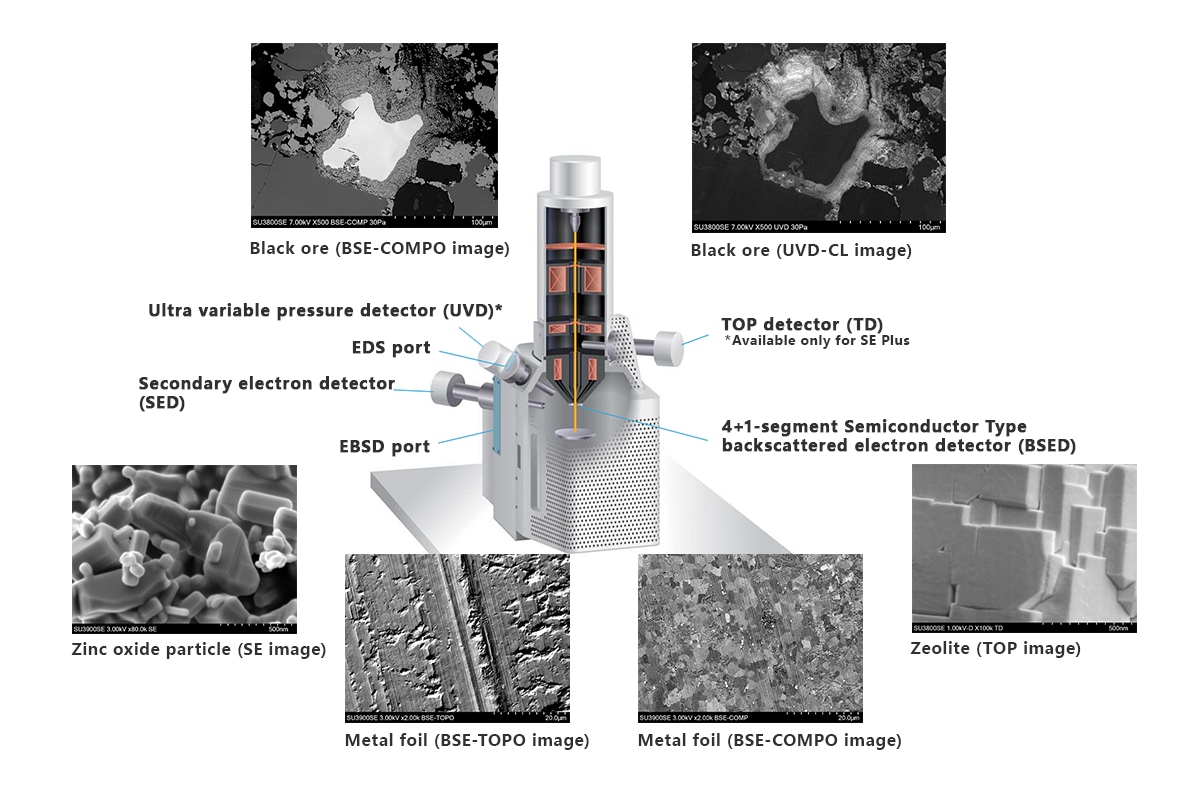
●High resolution for improved top-surface imaging
The resolution has been improved at both high and low accelerating voltages by adopting a newly developed Schottky electron gun. An advanced model (SE Plus) is also available to meet the demand for fine observation of top surface detail.
Furthermore, a low-accelerating-voltage high-sensitivity backscattered electron detector is included for obtaining composition and topographic information.
This makes it possible to perform a multifaceted analysis through acquisition of a wide range of information when combined with the optional ultra-variable-pressure detector (UVD).
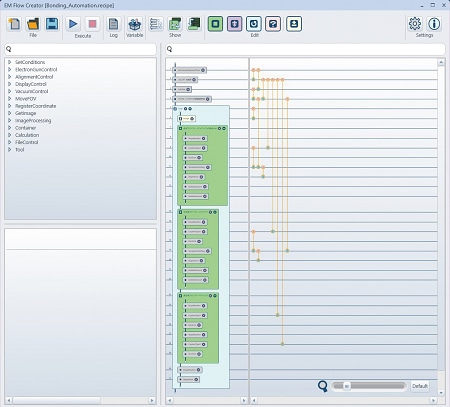
●Automation and support functions that improve usability
The SU3900SE/SU3800SE Series Microscopes are equipped with an automatic optical adjustment function that reduces manual work. This auto alignment sequence function eliminates the need to manually adjust the beam alignment, aperture alignment, focus, and stigmation. In addition, the EM Flow Creator is available to support automation of operations such as sequential image capture. A series of observation recipes can be created by setting parameters such as magnification, stage position, focus, and contrast adjustment, into blocks that can be combined, thus allowing the creation of customized recipes. Recipes can be created by dragging and dropping blocks into an arrangement like a flowchart. Automatic observation is possible by executing a created recipe.
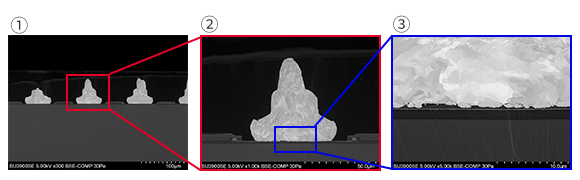
Specimen observation example(Metal wire bonding)
① Locate the area of interest and capture an image at x300.
② Execute the template matching function on image ① to locate a new area of interest. Then center on the location, zoom in, and capture an image at x1,000.
③ Execute the template matching function on image ② to locate a new area of interest. Then center on the location, zoom in, and capture an image at x5,000.
Applications Gallery
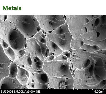
Fracture surface of iron wire
Microcavitation due to ductile failure can be seen.
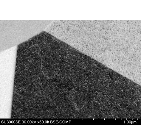
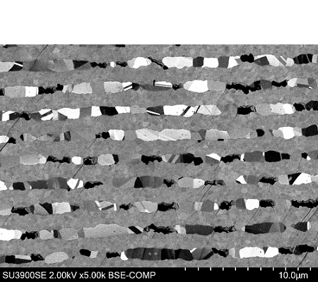
SUS316
Line-like contrast suggestive of dislocations can be seen.
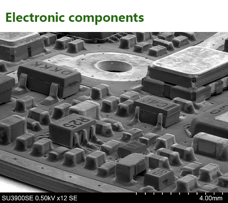
Printed circuit board
The 3D shapes and positions of mounted components can be seen using low magnification/high-tilt observation.
Cross section of layered ceramic capacitor
The composition and crystal contrast of nickel electrodes/dielectric layer can be observed.
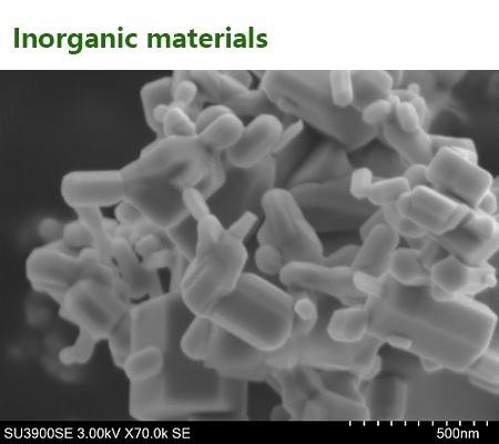
Zinc oxide particles
Fine particles with sizes of about 50 nm and 3D shape can be seen.
High-entropy carbide film
Distribution of particles with different compositions/shapes can be seen.
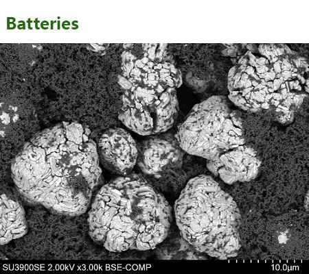
Lithium-ion battery cathode material
Distributions of cathode material particles and surrounding binder can be seen.
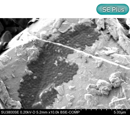
Lithium-ion battery anode material
lithium-ion battery anode material and binder is clearly distinguished using static voltage contrast.
Specifications
| Item | SU3900SE/SE Plus | SU3800SE/SE Plus | ||
|---|---|---|---|---|
| Electron Optics | Secondary Electron Image resolution | 0.9 nm@30 kV | ||
| 2.5 nm@1 kV | ||||
| 1.6 nm@1 kV (*1) (*2) | ||||
| Magnification | 5~600,000× | |||
| Electron Gun | ZrO/W Schottky Emitter | |||
| Accelerating Voltage | 0.5 kV~30 kV | |||
| Landing Voltage (*1) (*2) | 0.1 kV~2 kV | |||
| Probe Current | Max. 150 nA | |||
| Pressure Range | Variable Pressure (VP) mode | 6 to 150 Pa | ||
| Detectors | Standard Detectors | Secondary Electron Detector (SED) | ||
| TOP detector (TD) (*2) | ||||
| 41+1-segment Semiconductor Type Backscattered Electron Detector (BSED) | ||||
| Optional Detector (*3) | Ultra Variable Pressure Detector (UVD) | |||
| Specimen Stage | Stage Control | 5-axis Motor Drive | ||
| Movable Range | ||||
| X | 0~150 mm | 0~100 mm | ||
| Y | 0~150 mm | 0~50 mm | ||
| Z | 3~85 mm | 3~65 mm | ||
| T | -20~90° | |||
| R | 360° | |||
| Specimen Chamber | Mountable Specimen Size | Max. φ 300 mm | Max. φ 200 mm | |
*1 with deceleration mode
*2 available only for SE Plus specification
*3 Option
Citations
 Powered by Bioz
Related Information

Hitachi High-Tech Social Media


